High-Voltage ASICs

IC designers are typically trained in a world where a few volts are used and a couple 100mW or less is consumed. 12V starts to become high-voltage from an IC viewpoint, so what about 650V and 1.2kV in combination with power?
This knowledge and practice is built over the last decade with trial & error (illustrated with in-lab fireworks from time-to-time). Looking around, we can say we are one of the few teams that take on these challenges. Our track-record (700V on-chip regulators, 650V BLDC drivers and 1.2kV SiC drivers) confirms this and it’s good fun too.
We master the trade-offs combining high-performance analog and digital with high operating voltages. Thermal analysis and parasitic extraction, together with many years of experience, are key to our success.
Parasitic Extraction
Parasitics play a key role in high-voltage IC design. Parasitic capacitors can inject charge into high-impedant nodes - which can lead to crosstalk in sensitive analog, local overvoltages and worst case to oxide breakdown. Especially at high voltages, the current and power drawn from the supplies or internal nodes can become excessive, and needs to be well understood and designed for. Besides manual estimation based on the technology parameters, MinDCet engineers rely heavily on post-layout parasitic extraction ensuring robust first-time right designs.
Layout strategy
IC layout is an art, especially for high-performance high-voltage analog design. This art is mastered by our talented layout team:
- Adequate floor planning is key, taking into account package and PCB clearance and creepage requirements.
- The routing strategy takes into account the metal clearance and dielectric thicknesses for a given operating voltage.
- Understanding of parasitic field structures contributes to our success, avoiding (un-modeled) parasitic device turn-on or increased leakage currents.
Design Methodologies
- Process and options selection based on voltage, temperature, lifetime and cost/area requirements
- Design taking into account:
- Degradation mechanisms (TDDB, HCI, NBTI)
- Electromigration
- Lifetime requirements and mission profile
- Interconnect analysis :
- Proprietary design scripts
- FEM (Magwel, R3D)
- Thermal analysis :
- Proprietary design scripts
- FEA analysis (Magwel)
- Design of switched power systems
- Proprietary scripts for effciency/area optimization
- Proprietary scripts for loop analysis
- Design for reliability
- Bondability / packaging requirements
Use Case
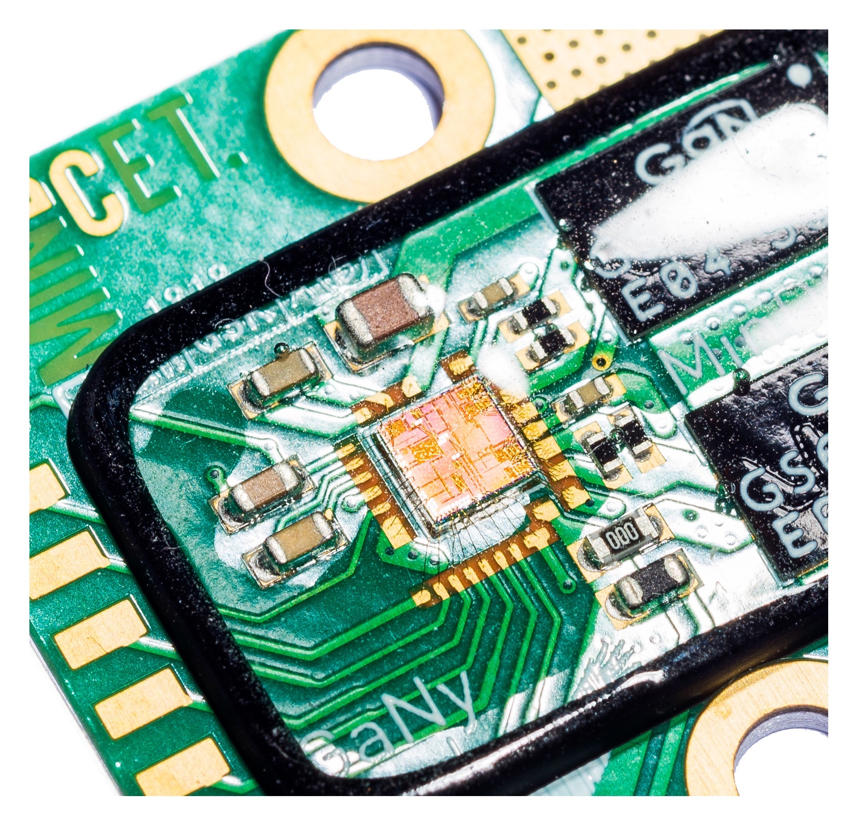
- Wide-bandgap gate drivers for SiC and GaN
- RF couplers
- Pin drivers for ATE
- MEMS drivers
- positioning
- electrostatic actuation
- ultrasound transducers


